I know I promised to write more advertising-related articles in 2014, but since everyone got so excited about the news that Google is going to make smart contact lenses, I figured it was OK if I wrote about a new way of making ultrathin, flexible and transparent electronics.
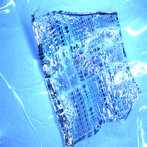
According to Hamish Johnston writing on physicsworld.com, the technique involves fabricating micron-thick electronic devices on a conventional silicon wafer, which is later detached by soaking it in water. The free-floating devices can then be placed onto a variety of biological tissues, including human skin and even a single hair. The technology could be used to make “smart” contact lenses for monitoring the pressure in an eyeball or for creating flexible solar cells. The new technique has been developed by Giovanni Salvatore and colleagues at the Swiss Federal Institute of Zurich (ETHZ), who have created transparent devices based on extremely thin and flexible transistors.
An important challenge for those wishing to incorporate electronics into biological systems is to make devices that are compatible with soft and flexible living tissue. Silicon – the material of choice in conventional electronics – is, unfortunately, strong and brittle, which makes it unsuitable for many biological applications. As a result, researchers have been busy developing devices based on more supple materials. The fabrication process begins with a conventional silicon wafer that is 2 inches (51 mm) in diameter. It is coated with two thin layers of two different water-soluble glues, one of which is polyvinyl acetate – the main component of the white glue used by schoolchildren and carpenters. A layer of parylene just 1 μm thick is then deposited on the top layer of glue. Electronic components are subsequently fabricated on the surface of the parylene by depositing semiconductor, dielectric and conducting materials in appropriate patterns. The resulting circuits are so thin that they lie less than 200 nm above the surface of the parylene itself. Although the researchers used metal conductors in some circuits, these were not completely transparent. So to make fully transparent transistors, the team turned to indium tin oxide, which is both optically transparent and an electrical conductor. Once the devices are built, the wafer is simply immersed in a dish of water. After about half an hour, the glue has dissolved and the film floats to the surface where it can be retrieved and cut into individual components.
One device made by the team is a differential amplifier with input and output electrodes, as well as an option to connect a power supply. The researchers operated the amplifier with the film both flat and bent; they found only a small degradation in performance in the latter configuration. In another study, a device comprising one thin-film transistor (TFT) was wrapped around a human hair, bending the TFT into a radius of curvature of just 50 μm. Despite the strain on the TFT, it was able to operate normally. The team also integrated a strain gauge into one of its devices, which was transferred to the surface of a contact lens. According to Salvatore, such a device could be used to provide real-time information about the pressure in an eyeball. He and his colleagues argue that such a system could offer significant improvements in the diagnosis of glaucoma. The researchers also showed that the flexible electronics could be stuck to a range of different surfaces, including human skin, a plant leaf and a number of different everyday materials, including textiles and rubber.
So far, all of the devices have been powered externally. But to be of practical use, devices need internal power supplies. Salvatore toldphysicsworld.com that the ETHZ group is now working on several different schemes for supplying energy to the devices. One option borrows from passive RFID tags, which are used to identify and track goods and even people. In the case of a contact-lens-mounted device, an radio-frequency (RF) signal is sent to the device and absorbed by a built-in antenna. This gives the sensor enough energy to read the strain gauge and then broadcast the result as an RF signal. The team is also exploring how solar energy could be used to power devices.


